
Welcome to SetupAndHold.com, where we unravel the mysteries of technology, one story at a time. Today, we’re diving into the fascinating (and sometimes daunting) world of ASIC design. Think of this as the opening scene of an epic tale, where we’ll meet the key characters (aka the steps in the design flow) and set the stage for future adventures. Ready? Let’s begin!
Defining the Mission – Specification
Every great story starts with a plan, and ASIC design is no different. Our hero, the Designer, sits down to answer the big questions:
- What is this chip supposed to do? (Functional specs, please!)
- How fast, how small, and how power-efficient should it be? (Constraints, constraints!)
- How much time and money do we have? (Because, let’s be real, resources matter.)
This is the Specification Phase, where dreams are put on paper. But beware! A vague plan here can lead to chaos later. For example, failing to define accurate power budgets or timing constraints can result in a chip that either doesn’t meet performance targets or consumes too much energy. Tools like MATLAB or SystemC are often used to model system behavior and validate specifications before moving forward.
Sketching the Blueprint – Architectural Design
With the plan in hand, the Designer sketches the architecture. This is where the chip’s soul takes shape. Key decisions include:
- What functional blocks are needed? (A CPU? Memory? Some fancy accelerators?)
- How will they communicate? (Buses, interconnects, and handshakes, oh my!)
- What’s the trade-off between performance and power efficiency?
This phase is like designing a city before building it—defining neighborhoods (functional blocks), roads (data paths), and traffic rules (protocols). For example, in a video-coding ASIC, the architecture must ensure that the encoder block can process UHD@60fps without bottlenecks. Tools like Cadence Stratus or Synopsys Platform Architect help simulate and optimize these high-level designs.
Writing the Hardware Story – RTL Design
Now comes the RTL Design Phase, where the Designer writes code in a hardware description language (HDL) like Verilog or VHDL. Unlike software, this code describes hardware structures—registers, logic gates, and data paths.
But writing code isn’t enough. Our hero must also battle bugs in the Verification Phase. Using testbenches and simulations, they ensure the design behaves as expected. (Spoiler: It never does on the first try.) Advanced techniques like formal verification and coverage-driven testing are essential to catch corner cases. A poorly verified design might fail to handle rare timing conditions, leading to catastrophic errors in the final chip.
Turning Code into Gates – Logical Synthesis
Next, the RTL code undergoes a magical transformation called Synthesis. Tools like Synopsys Design Compiler act as the wizard’s spellbook, converting RTL into a netlist—a list of logic gates and connections representing the actual hardware. But here’s the trick: synthesis follows a ‘rulebook’ called the SDC file (Synopsys Design Constraints), which defines timing constraints like clock speed and input delays.
Additionally, engineers insert hidden Design for Test (DFT) structures, such as scan chains, during synthesis—think of them as secret tunnels that allow testing every register after fabrication. Without these, debugging a manufactured chip would be like solving a puzzle blindfolded!
Building the Silicon City – Physical Design
Now things get physical! The netlist is mapped onto silicon in the Physical Design Phase, which involves:
- Floorplanning: Deciding where everything goes. (Think of it as arranging furniture in a tiny apartment.)
- Placement: Positioning each gate optimally to balance performance and power.
- Routing: Connecting everything with microscopic wires. (Traffic management at the nanoscale!)
Some teams create hard macros—pre-optimized blocks, like LEGO pieces, that can be reused across designs. Others take a full-chip approach, carefully defining everything from scratch. Tools like Cadence Innovus or Synopsys IC Compiler automate these tasks, but challenges like signal integrity and thermal management require careful manual intervention. Improper routing can lead to crosstalk, where signals interfere with each other, causing errors.
Testing the Foundations – Verification & Signoff
Before the chip can be sent for fabrication, it must pass a final verification process:
- LVS (Layout vs. Schematic): Ensures the layout matches the intended design.
- DRC (Design Rule Checking): Ensures the chip follows foundry manufacturing rules.
- LEC (Logical Equivalence Check): Ensures no functional errors were introduced during synthesis.
- STA (Static Timing Analysis): Ensures that all signal paths meet timing constraints.
Skipping these checks could result in a multi-million-dollar disaster if the fabricated chip doesn’t function correctly!
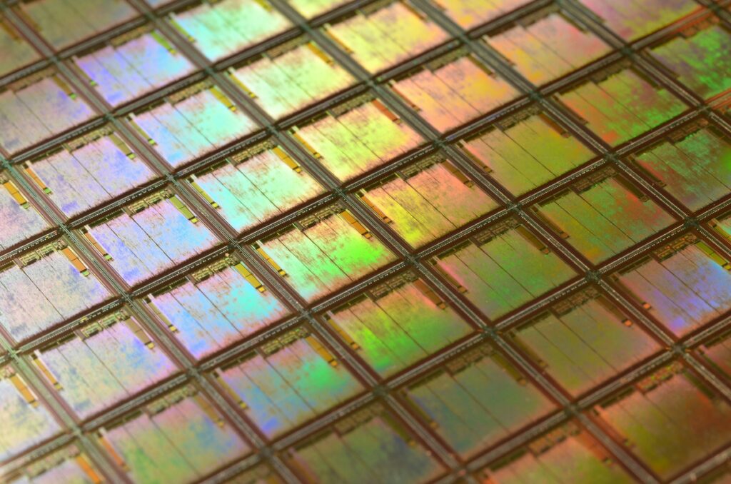
From Design to Reality – Fabrication & Manufacturing
With all checks passed, the design is sent to a foundry, where it’s transformed into a physical chip. This is the Fabrication Phase, where silicon wafers are etched, doped, and layered to create the final product. Foundries like TSMC or Intel use advanced processes such as FinFET and EUV lithography to achieve nanometer-scale precision.
After fabrication, the chips are tested using Automated Test Equipment (ATE) and scan chains to detect manufacturing defects. Only after passing these tests can the chip be integrated into products like smartphones, data centers, or automotive systems.
Epilogue – The Journey Has Just Begun
And there you have it—the ASIC design flow in a nutshell! But this is just the beginning. In future posts, we’ll dive deeper into each chapter, exploring the tools, techniques, and challenges that make ASIC design such a thrilling adventure.
See you in the next post, where we’ll continue unraveling the exciting world of ASICs!